Electronic measurements with nm resolution
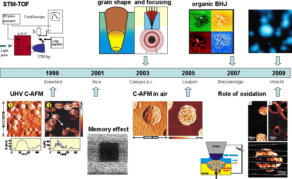
In order to understand the operation of devices based on nanostructures, we need to measure the electronic properties with nanometer resolution. Such experiments can be done using the scanning probe microscopes. The timeline shows the main milestones of our research as reported at the ICANS conferences:

|
The main tool for our research is the conductive atomic force microscopy (C-AFM), where a shart tip of the AFM traces the surface in contact mode and at the same time measures the local conductivity with resolution down to few nanometers. |
| The first results allowed us to detect grains of different sizes and to follow the internal structure of the larger grains. The measurements were done in ultra high vacuum in order to limit the oxidation of silicon surface. |
 |
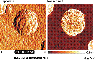
The next step was the transfer of the measurements to ambient AFM and modification necessary for the layers covered by a layer of native oxide. In this case we needed to increase the sensitivity of the current detection. |
 |
| Later we discovered that the measurement process itself can modify the surface by local anodic oxidation. The oxidation occurs due to the presence of water meniscus at the tip-surface junction. The oxyanions driven through the oxide by the applied electrical field oxidize the underlying silicon. The tip leaves behind an oxidized path which an influence the C-AFM maps. |
 |