The group builds on its tradition of research of silicon thin films (either amorphous or with nanocrystalline or microcrystalline structure) and newly also on silicon nanostructures. |
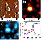
The understanding of physical properties of Si nanostructures requires high resolution, provided by the scanning probe methods. We use conductive atomic force microscopy to measure the structure and local electronic properties, together with Raman microspectroscopy to probe the structure. |
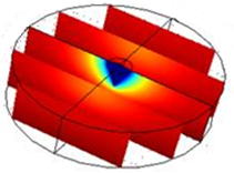
Experimental data were the basis for formulating a phenomenological model of transport in nanostructured silicon films. Further modelling based on computation of internal fields by finite element method is in progress. |
 |
 |
 |